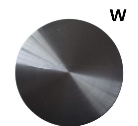
Tungsten Sputtering Target — 99.95% (3N5) PVD Grade
High-purity tungsten (W) sputtering target for semiconductor diffusion barrier layers, X-ray tube anodes, hard coating research, and high-temperature refractory thin-film deposition. Tungsten is the standard metallization material for contact plug fill in advanced semiconductor nodes (VLSI/ULSI).
Key Specifications
- Purity: 99.95% W (3N5) or 99.9% (3N)
- Relative density: ≥97%
- Grain size: <100 µm (fine grain for uniform deposition)
- Geometry: Disc 2″–8″ or rectangular, custom sizes
- Thickness: 3–12 mm
Applications
- Semiconductor W contact plug (VLSI metallization)
- Diffusion barrier layer (W-TiN stack)
- X-ray tube anode target
- Hard coating research (WC, W₂C)
Specify geometry, purity grade, and backing plate type for quotation. Lead time typically 7–14 business days for standard sizes.